キャッシュ設定の調査
2017年7月、Raspberry Pi3のキャッシュメモリはどんな構造になっているか興味があり調べてみました。
先日、Raspberry Pi2のキャッシュについて調査しました。キャッシュの基本的な説明と調査方法については、こちらのブログを参照してください。
Raspberry Pi3のキャッシュ構成は?
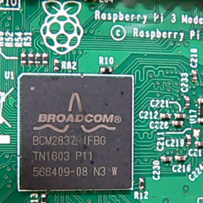
公式サイトのドキュメントをみると、Raspberry Pi3は、Broadcom社のBCM2837というチップを使用しています。
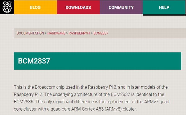
BCM2837
Broadcom BCM2837
BCM2837
This is the Broadcom chip used in the Raspberry Pi 3, and in later models of the Raspberry Pi 2. The underlying architecture of the BCM2837 is identical to the BCM2836. The only significant difference is the replacement of the ARMv7 quad core cluster with a quad-core ARM Cortex A53 (ARMv8) cluster.
【要約】
BCM2837チップは、Raspberry Pi3とそれ以降のRaspberry Pi2で使用しています。
BCM2837の基本アーキテクチャはBCM2836と同じです。
唯一の大きな違いは、ARMv7クアッドコアクラスタをクアッドコアARM Cortex A53(ARMv8)クラスタに置き換えることです。
今まで知りませんでしたが、Raspberry Pi3と同じ Cortex-A53を搭載しているRaspberry Pi2があるそうです。
BCM2836は、4つのCPUコアを持つCortex-A53(ARMv8)を搭載しています。

Cortex-A53
4つのCPUコア内部に命令キャッシュ(L1 I-Cache)とデータキャッシュ(L1 D-Cache)があり、メモリとの間に統合キャッシュ(L2 Cache)があります。
ARMサイトの「Cortex-A53 MPCore Technical Reference Manual」を参考にします。
Cortex-A53 Manual
L1 memory system
LEVEL1のメモリシステムについて調べます。
6.1. About the L1 memory system
The L1 memory system consists of separate instruction and data caches. The implementer configures the instruction and data caches independently during implementation, to sizes of 8KB, 16KB, 32KB, or 64KB.
The L1 Instruction memory system has the following key features:
・Instruction side cache line length of 64 bytes.
・2-way set associative L1 Instruction cache.
・128-bit read interface to the L2 memory system.Data side cache line length of 64 bytes.
・4-way set associative L1 Data cache.
・256-bit write interface to the L2 memory system.
・128-bit read interface to the L2 memory system.
・Read buffer that services the Data Cache Unit (DCU), the Instruction Fetch Unit (IFU) and the TLB.
・64-bit read path from the data L1 memory system to the datapath.
・128-bit write path from the datapath to the L1 memory system.
・Support for three outstanding data cache misses.
・Merging store buffer capability. This handles writes to: Device memory, Normal Cacheable memory, Normal Non-cacheable memory.
・Data side prefetch engine.
L1メモリシステムは、独立した命令キャッシュとデータキャッシュで構成しています。実装時に、命令キャッシュとデータキャッシュをそれぞれ 8KB、16KB、32KB、64KBのサイズに構成できます。
L1命令キャッシュは、2ウェイセットアソシアティブ構造で、キャッシュライン長は64バイトです。(Cortex-A7は、32バイトです)
L1データキャッシュは、4ウェイセットアソシアティブ構造で、キャッシュライン長は64バイトです。
L2 memory system
LEVEL2のメモリシステムについて調べます。
7.1. About the L2 Memory system
The L2 memory system consists of an:
● Integrated Snoop Control Unit (SCU), connecting up to four cores within a cluster. The SCU also has duplicate copies of the L1 Data cache tags for coherency support. The L2 memory system interfaces to the external memory system with either an AMBA 4 ACE bus or an AMBA 5 CHI bus. All bus interfaces are 128-bits wide.
● Optional tightly-coupled L2 cache that includes:
・Configurable L2 cache size of 128KB, 256KB, 512KB, 1MB and 2MB.
・Fixed line length of 64 bytes.
・Physically indexed and tagged cache.
・16-way set-associative cache structure.
・Optional ACP interface if an L2 cache is configured.
・Optional ECC protection.
L2キャッシュサイズは、128KB、256KB、512KB、1MB、2MBに設定できます。
L2キャッシュは、16ウェイセットアソシアティブ構造で、キャッシュライン長は64バイトです。
キャッシュ構成を調べる
キャッシュ構成は、セットアソシアティブ構造ということがわかりました。しかし、キャッシュサイズなどは実装時に設定できるようですので、使用するOSの設定などにより変わってきます。
RaspbianのLinuxで実際のキャッシュ構成を調べてみます。
OSバージョンを下記に示します。ファームウェアバージョンは#1013です。
pi@pi3:~ $ uname -a
Linux pi3 4.9.34-v7+ #1013 SMP Sun Jun 25 17:06:40 BST 2017 armv7l GNU/Linux

pi@pi3:~ $ lsb_release -a
No LSB modules are available.
Distributor ID: Raspbian
Description:    Raspbian GNU/Linux 8.0 (jessie)
Release:        8.0
Codename:       jessie
キャッシュ情報を参照する cacheinfo.c は、下記ブログで作成したプログラムコードを使用します。
カーネルモジュールの実行
カーネルモジュールをロードします。
# insmod cachemod.ko
カーネルバッファにメッセージを記録したことを確認します。
# dmesg |tail -6
[  120.615337] Start Cache Info
[  120.615357] CTR reg=84448004
[  120.615375] CLIDR reg=0a200023
[  120.615383] CCSIDR  DATA L1 CACHE 700fe01a
[  120.615391] CCSIDR  INST L1 CACHE 201fe00a
[  120.615400] CCSIDR  UNIF L2 CACHE 703fe07a
カーネルモジュールをアンロードします。
# rmmod cachemod
キャッシュ情報取得結果
Cache Type Register
CTR(Cache Type Register)を参照すると 0x84448004 となりました。
[CTR説明]
- CWG : Cache Write-Back granule. Log2 of the number of words of the maximum size of memory that can be overwritten as a result of the eviction of a cache entry that has had a memory location in it modified
- ERG : Exclusives Reservation Granule. Log2 of the number of words of the maximum size of the reservation granule that has been implemented for the Load-Exclusive and Store-Exclusive instructions
- DminLine : Log2 of the number of words in the smallest cache line of all the data and unified caches that the processor controls
- L1Ip : L1 instruction cache policy. Indicates the indexing and tagging policy for the L1 instruction cache
- IminLine : Log2 of the number of words in the smallest cache line of all the instruction caches that the processor controls
| Field | Value | Function |
|---|---|---|
| CWG | 0x4 | Cache Write-Back granule size is 16 words |
| ERG | 0x4 | Exclusive reservation granule size is 16 words |
| DminLine | 0x4 | Smallest data cache line size is 16 words |
| L1Ip | b10 | Virtually Indexed Physically Tagged (VIPT) |
| IminLine | 0x4 | Smallest instruction cache line size is 16 words |
Cache Level ID Register
CLIDR(Cache Level ID Register)を参照すると 0x0a200023 となりました。
[CLIDR説明]
- LoUU : Indicates the Level of Unification Uniprocessor for the cache hierarchy
- LoC : Indicates the Level of Coherency for the cache hierarchy
- LoUIS : Indicates the Level of Unification Inner Shareable for the cache hierarchy
- Ctype3 : Indicates the type of cache if the processor implements level 3 cache
- Ctype2 : Indicates the type of cache if the processor implements level 2 cache
- Ctype1 : Indicates the type of cache implemented at level 1
| Field | Value | Function |
|---|---|---|
| LoUU | 0x1 | L2 cache |
| LoC | 0b010 | L2 cache coherency |
| LoUIS | 0b001 | L2 cache |
| Ctype3 | 0b000 | L3 cache not implemented. |
| Ctype2 | 0b100 | Unified instruction and data caches. |
| Ctype1 | 0b011 | Separate instruction and data caches |
Level1 キャッシュは、分離した命令キャッシュとデータキャッシュがあります。Level2キャッシュは、命令とデータを統合したキャッシュがあります。
Cache Size Selection Register
CSSELR(Cache Size Selection Register)は、CCSIDR(Cache Size ID Register)を選択します。
[CSSELR説明]
| Field | Value | Function |
|---|---|---|
| Level | Cache level of required cache | |
| 0b000 | Level 1 | |
| 0b001 | Level 2 | |
| InD | Instruction not Data bit | |
| 0 | Data or unified cache | |
| 1 | Instruction cache |
プログラムでは、3つのキャッシュを指定してキャッシュサイズを取得しています。
- Level 1 Data Cache
- Level 1 Instruction Cache
- Level 2 Unified Cache
Cache Size ID Register
CCSIDR(Cache Size ID Register)を参照すると、以下のようになりました。
| Cache Selection | Value |
|---|---|
| Level 1 Data Cache | 700fe01a |
| Level 1 Instruction Cache | 201fe00a |
| Level 2 Unified Cache | 703fe07a |
[CCSIDR説明]
| Field | Value | Function |
|---|---|---|
| WT | Indicates support for Write-Through | |
| 0 | Cache level does not support Write-Throug | |
| 1 | Cache level supports Write-Through | |
| WB | Indicates support for Write-Back | |
| 0 | Cache level does not support Write-Back | |
| 1 | Cache level supports Write-Back | |
| RA | Indicates support for Read-Allocation | |
| 0 | Cache level does not support Read-Allocation | |
| 1 | Cache level supports Read-Allocation | |
| WA | Indicates support for Write-Allocation | |
| 0 | Cache level does not support Write-Allocation | |
| 1 | Cache level supports Write-Allocation | |
| NumSets | Indicates the number of sets in cache – 1 | |
| Associativity | Indicates the associativity of cache – 1 | |
| LineSize | Indicates the cache line | |
| 0b001 | 8 words per line | |
| 0b010 | 16 words per line |
Level 1 Data Cache は、WB,RA,WA をサポートしています。
| Field | Value | Function |
|---|---|---|
| NumSets | 0x7F | 128 sets |
| Associativity | 0x03 | 4-ways |
| LineSize | 0x2 | 16 words per line |
Level 1 Data Cacheのサイズは、Line Size(16word) × sets(128) × ways(4) = 32KB となります。
Level 1 Instruction Cache は、RA をサポートしています。
| Field | Value | Function |
|---|---|---|
| NumSets | 0x0FF | 256 sets |
| Associativity | 0x01 | 2-ways |
| LineSize | 0x2 | 16 words per line |
Level 1 Instruction Cacheのサイズは、Line Size(16word) × sets(256) × ways(2) = 32KB となります。
Level 2 Unified Cache は、WB,RA,WA をサポートしています。
| Field | Value | Function |
|---|---|---|
| NumSets | 0x1FF | 512 sets |
| Associativity | 0x0F | 16-ways |
| LineSize | 0x2 | 16 words per line |
Level 2 Unified Cacheのサイズは、Line Size(16word) × sets(512) × ways(16) = 512KB となります。
BCM2836(Pi2)とBCM2837(Pi3)の比較
調査結果からBCM2836(Pi2)とBCM2837(Pi3)のキャッシュ構成を比較します。
| Cache種別 | BCM2836(Pi2) | BCM2837(Pi3) |
|---|---|---|
| L1 Data | Line Size(16word) sets(128)×ways(4) 32KB |
Line Size(16word) sets(128)×ways(4) 32KB |
| L1 Inst | Line Size(8word) sets(512)×ways(2) 32KB |
Line Size(16word) sets(256)×ways(2) 32KB |
| L2 Unified | Line Size(16word) sets(1024)×ways(8) 512KB |
Line Size(16word) sets(512)×ways(16) 512KB |
キャッシュサイズは、両者ともに同じサイズです。しかし、キャッシュ構成が少々異なりました。
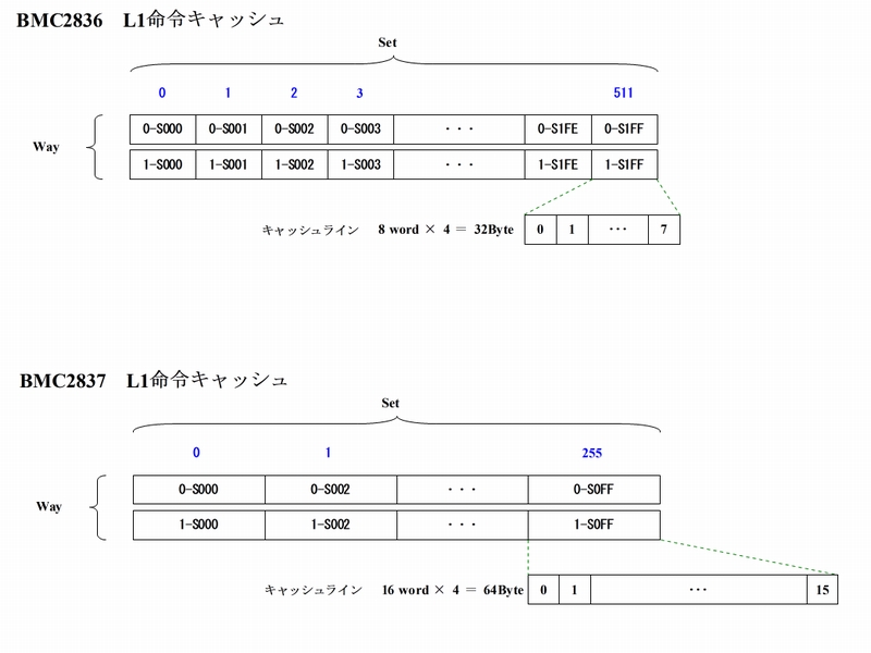
L1命令キャッシュ 比較
L1命令キャッシュは、Line Sizeが倍の16wordになりましたが、セット数が半分の256になりました。
キャッシュのフェッチ単位が8word→16wordと大きくなりました。命令フェッチは分岐命令がない限り連続するので、キャッシュ効率が良くなります。

L2統合キャッシュ 比較
L2統合キャッシュは、セット数が半分の512になりましたが、ウェイが倍の16になりました。ウェイ数が増加したので、キャッシュマッピングの自由度が増加しました。
まとめ
Raspberry Pi3のRaspbian OSのキャッシュメモリ構造を調べました。
- Level 1 Data Cacheは、16wordライン長で4-Way 128セットアソシアティブ構造で32KB搭載しています。
- Level 1 Instruction Cacheは、16wordライン長で2-Way 256セットアソシアティブ構造で32KB搭載しています。
- Level 2 Unified Cacheは、16wordライン長で16-Way 512セットアソシアティブ構造で512KB搭載しています。
さて、最適化実装する場合はどんな点に留意すれば良いでしょうか?またの機会に考えてみます。
Raspberry Pi2 (BMC2836)と Raspberry Pi3 (BMC2837)で最適化実装するとき、両者に同じ手法が効率的に働くのでしょうか?またの機会に考えてみます。