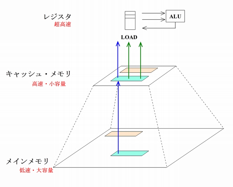
キャッシュメモリとは
2017年7月、Raspberry Pi2のキャッシュメモリはどんな構造になっているか興味があり調べてみました。
Raspberry Pi2のCPU動作周波数は900MHzと高く1クロックは約1nsとなります。CPU内のレジスタ間演算は数nsと高速であるのに比べ、SDRAMメモリのアクセス速度は数十ns程度です。キャッシュメモリは、CPU演算とメモリアクセスの速度差を縮めるためにCPUとメインメモリの間に配置した高速なメモリです。
キャッシュの概念
一般的に、あるデータを参照するときにそのデータの近辺を参照する可能性が非常に高いという「プログラムの局所性」があります。メインメモリから読み込んだデータを高速なキャッシュメモリに蓄えておき、次に近辺へのアクセスがあった場合はキャッシュメモリから読み込むことにより高速にアクセスすることができるわけです。
Raspberry Pi2のメインメモリ容量は1GBと大容量なのに比べ、キャッシュメモリ容量は32KBと小容量です。従って、頻繁にアクセスするメモリの一部分をキャッシュメモリに一時的に蓄える仕組みとなっています。キャッシュに存在しないアドレスのメモリアクセスはキャッシュ・ミスヒットが発生します。最初にメインメモリからキャッシュメモリにキャッシュ・ライン分のデータを読み込み、次にキャッシュメモリから該当アドレスのデータを読み込みます。
ソフトウェアをマイクロプロセッサ向けに最適化実装する場合は、キャッシュ・ヒットが向上するようにデータのアクセス方法を工夫します。そのときキャッシュ構造の理解がとても重要になります。
Raspberry Pi2のキャッシュ構成は?
公式サイトのドキュメントをみると、Raspberry Pi2はBroadcom社のBCM2836というチップを使用しています。
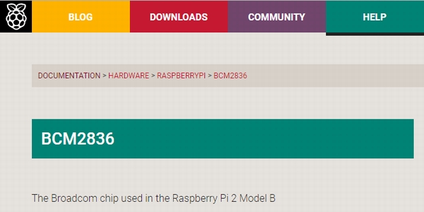
BCM2836
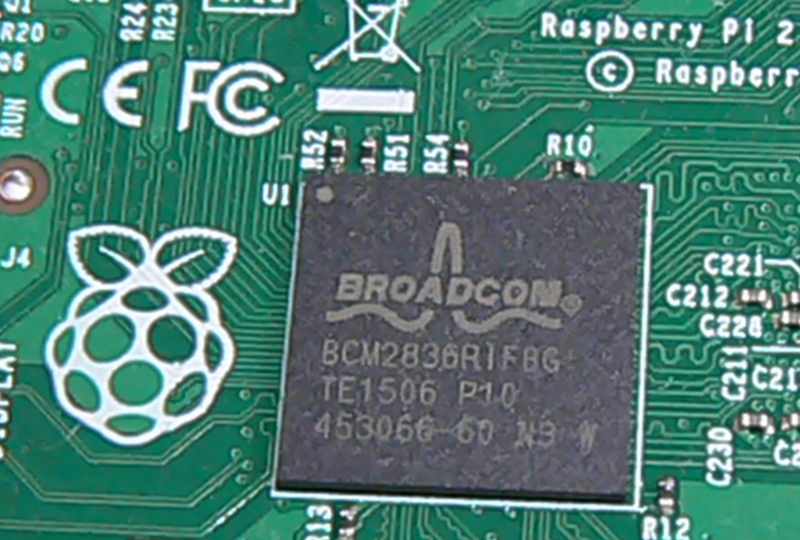
Broadcom BCM2836
BCM2836は、4つのCPUコアを持つCortex-A7を搭載しています。

Cortex-A7
4つのCPUコア内部に命令キャッシュ(L1 I-Cache)とデータキャッシュ(L1 D-Cache)があり、メモリとの間に統合キャッシュ(L2 Cache)があります。
ARMサイトの「Cortex-A7 MPCore Technical Reference Manual」を参考にします。
Cortex-A7 Manual
L1 memory system
LEVEL1のメモリシステムについて調べます。
6.1. About the L1 memory system
The L1 memory system consists of separate instruction and data caches. You can configure the instruction and data caches independently during implementation to sizes of 8KB, 16KB, 32KB, or 64KB.
The L1 memory system has a store buffer that has four 64-bit slots with data merging capability. It handles writes to Device, Strongly-ordered, Cacheable and Non-cacheable memory.The L1 instruction memory system has the following features:
・Instruction side cache line length of 32-bytes.
・Virtually indexed and physically tagged instruction cache.
・Pseudo random cache replacement policy.
・2-way set-associative instruction cache.
・Support for four sizes of memory page.
・Export of memory attributes for external memory systems.
・Support for Security Extensions.
・Can be disabled independently, using the system control coprocessor. See System Control Register
・On a cache miss, critical word first filling of the cache is performedThe L1 data memory system has the following features:
・Data side cache line length of 64-bytes.
・Physically indexed and physically tagged data cache.
・Pseudo random cache replacement policy.
・4-way set-associative data cache.
・Two 32-byte linefill buffers and one 64-byte eviction buffer.
・A 4-entry, 64-bit merging store buffer.
・Can be disabled independently, using the system control coprocessor. See System Control Register.
・On a cache miss, critical word first filling of the cache is performed.
L1メモリシステムは、独立した命令キャッシュとデータキャッシュで構成しています。実装時に、命令キャッシュとデータキャッシュをそれぞれ 8KB、16KB、32KB、64KBのサイズに構成できます。
L1命令キャッシュは、2ウェイセットアソシアティブ構造で、キャッシュライン長は32バイトです。
L1データキャッシュは、4ウェイセットアソシアティブ構造で、キャッシュライン長は64バイトです。
L2 memory system
LEVEL2のメモリシステムについて調べます。
7.1. About the L2 Memory system
The L2 memory system consists of an:
● Integrated Snoop Control Unit (SCU), connecting up to four processors within a cluster. The SCU also has duplicate copies of the L1 data cache directories for coherency support. The L2 memory system interfaces with an AMBA AXI Coherency Extension (ACE) interconnect on a 128-bit wide bus.
● Optional tightly-coupled L2 cache that includes:
・Configurable L2 cache size of 128KB, 256KB, 512KB, and 1MB.
・Fixed line length of 64 bytes.
・Physically indexed and tagged cache.
・8-way set-associative cache structure.
・Pseudo-random cache replacement policy.
L2キャッシュサイズは、128KB、256KB、512KB、1MBに設定できます。
L2キャッシュは、8ウェイセットアソシアティブ構造で、キャッシュライン長は64バイトです。
キャッシュ構成を調べる
キャッシュ構成は、セットアソシアティブ構造ということがわかりました。しかし、キャッシュサイズなどは実装時に設定できるようですので、使用するOSの設定などにより変わってきます。
RaspbianのLinuxで実際のキャッシュ構成を調べてみます。
OSバージョンを下記に示します。ファームウェアバージョンは#1013です。
pi@pi2:~ $ uname -a
Linux pi2 4.9.34-v7+ #1013 SMP Sun Jun 25 17:06:40 BST 2017 armv7l GNU/Linux

pi@pi2:~ $ lsb_release -a
No LSB modules are available.
Distributor ID: Raspbian
Description:    Raspbian GNU/Linux 8.0 (jessie)
Release:        8.0
Codename:       jessie
システム制御コプロセッサ(CP15)にキャッシュ情報を取得するレジスタがあります。
| Name | Description | CRn | Op1 | CRm | Op2 |
|---|---|---|---|---|---|
| CTR | Cache Type Register | c0 | 0 | c0 | 1 |
| CCSIDR | Cache Size ID Register | c0 | 1 | c0 | 0 |
| CLIDR | Cache Level ID Register | c0 | 1 | c0 | 0 |
| CSSELR | Cache Size Selection Register | c0 | 2 | c0 | 0 |
これらのレジスタにアクセスするには特権レベルが必要ですのでカーネルモジュールとして作成しました。
カーネルモジュールの作成方法については、「Raspberry Piでカーネルモジュールを作成」を参照してください。
キャッシュ情報参照プログラムコード
キャッシュ情報を参照する cacheinfo.c プログラムコードを下記に示します。
pi@pi2:~ $ cat cacheinfo.c
#include <linux/module.h>
#include <linux/init.h>

#define CSSELR_InD_INST (1)
#define CSSELR_InD_DATA (0)
#define CSSELR_LEVEL_L1 ((00)<<1)
#define CSSELR_LEVEL_L2 ((01)<<1)

MODULE_LICENSE("Dual BSD/GPL");

static int cacheinfo_init(void)
{
     unsigned long reg;
     unsigned long  csselr;

     printk(KERN_ALERT "Start Cache Info \n");

     asm volatile("mrc p15 ,0 ,%0 ,c0 ,c0 ,1" : "=r" (reg));
     printk(KERN_ALERT "CTR reg=%08lx\n",reg);

     asm volatile("mrc p15 ,1 ,%0 ,c0 ,c0 ,1" : "=r" (reg));
     printk(KERN_ALERT "CLIDR reg=%08lx\n",reg);

     csselr = CSSELR_InD_DATA | CSSELR_LEVEL_L1 ;
     asm volatile("mcr p15 ,2 ,%0 ,c0 ,c0 ,0" :: "r" (csselr));
     asm volatile("mrc p15 ,1 ,%0 ,c0 ,c0 ,0" : "=r" (reg));
     printk(KERN_ALERT "CCSIDR  DATA L1 CACHE %08lx\n",reg);

     csselr = CSSELR_InD_INST | CSSELR_LEVEL_L1 ;
     asm volatile("mcr p15 ,2 ,%0 ,c0 ,c0 ,0" :: "r" (csselr));
     asm volatile("mrc p15 ,1 ,%0 ,c0 ,c0 ,0" : "=r" (reg));
     printk(KERN_ALERT "CCSIDR  INST L1 CACHE %08lx\n",reg);

     csselr = CSSELR_InD_DATA | CSSELR_LEVEL_L2 ;
     asm volatile("mcr p15 ,2 ,%0 ,c0 ,c0 ,0" :: "r" (csselr));
     asm volatile("mrc p15 ,1 ,%0 ,c0 ,c0 ,0" : "=r" (reg));
     printk(KERN_ALERT "CCSIDR  UNIF L2 CACHE %08lx\n",reg);

     return 0;
}

static void cacheinfo_exit(void)
{
     printk(KERN_ALERT "End Cache Info \n");
}

module_init(cacheinfo_init);
module_exit(cacheinfo_exit);
カーネルモジュールのビルド
Makefileを作成します。
pi@pi2:~ $ cat Makefile
KERNEL_DIR = /lib/modules/$(shell uname -r)/build

obj-m := cachemod.o

cachemod-objs := cacheinfo.o

all:
	make -C $(KERNEL_DIR) M=$(PWD) modules

clean:
	make -C $(KERNEL_DIR) M=$(PWD) clean
カーネルモジュールをビルドします。ルート権限が必要なのでスーパーユーザーでmakeします。
pi@pi2:~ $ sudo su
# make
make -C /lib/modules/4.9.34-v7+/build  M=/home/pi/myHome/cp15/cacheInfo modules
make[1]: Entering directory '/root/linux-3e22e20f80899847293ef835b083e36ecb866d2d'
  CC [M]  /home/pi/myHome/cp15/cacheInfo/cacheinfo.o
  LD [M]  /home/pi/myHome/cp15/cacheInfo/cachemod.o
  Building modules, stage 2.
  MODPOST 1 modules
  CC      /home/pi/myHome/cp15/cacheInfo/cachemod.mod.o
  LD [M]  /home/pi/myHome/cp15/cacheInfo/cachemod.ko
make[1]: Leaving directory '/root/linux-3e22e20f80899847293ef835b083e36ecb866d2d'
カーネルモジュール cachemod.ko の情報を表示します。
# modinfo cachemod.ko
filename:       /home/pi/myHome/cp15/cacheInfo/cachemod.ko
license:        Dual BSD/GPL
srcversion:     D9480FE2406A98F24C3B1C8
depends:
vermagic:       4.9.34-v7+ SMP mod_unload modversions ARMv7 p2v8
カーネルモジュールの実行
カーネルモジュールをロードします。
# insmod cachemod.ko
カーネルバッファにメッセージを記録したことを確認します。
# dmesg |tail -6
[  785.385682] Start Cache Info
[  785.388681] CTR reg=84448003
[  785.394852] CLIDR reg=0a200023
[  785.397908] CCSIDR  DATA L1 CACHE 700fe01a
[  785.402057] CCSIDR  INST L1 CACHE 203fe009
[  785.406160] CCSIDR  UNIF L2 CACHE 707fe03a
カーネルモジュールをアンロードします。
# rmmod cachemod
キャッシュ情報取得結果
Cache Type Register
CTR(Cache Type Register)を参照すると 0x84448003 となりました。
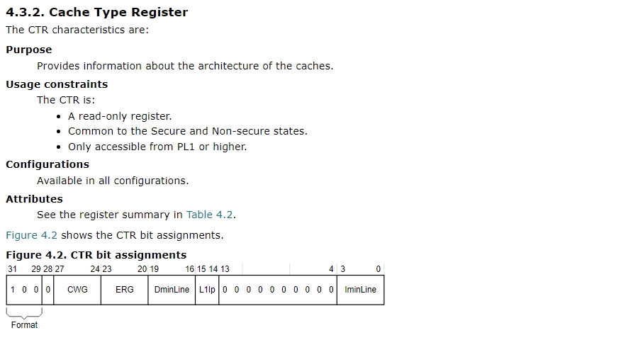
CTR説明
- CWG : Cache Write-Back granule. Log2 of the number of words of the maximum size of memory that can be overwritten as a result of the eviction of a cache entry that has had a memory location in it modified
- ERG : Exclusives Reservation Granule. Log2 of the number of words of the maximum size of the reservation granule that has been implemented for the Load-Exclusive and Store-Exclusive instructions
- DminLine : Log2 of the number of words in the smallest cache line of all the data and unified caches that the processor controls
- L1Ip : L1 instruction cache policy. Indicates the indexing and tagging policy for the L1 instruction cache
- IminLine : Log2 of the number of words in the smallest cache line of all the instruction caches that the processor controls
| Field | Value | Function |
|---|---|---|
| CWG | 0x4 | Cache Write-Back granule size is 16 words |
| ERG | 0x4 | Exclusive reservation granule size is 16 words |
| DminLine | 0x4 | Smallest data cache line size is 16 words |
| L1Ip | b10 | Virtually Indexed Physically Tagged (VIPT) |
| IminLine | 0x3 | Smallest instruction cache line size is 8 words |
Cache Level ID Register
CLIDR(Cache Level ID Register)を参照すると 0x0a200023 となりました。
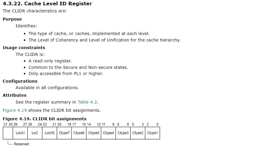
CLIDR説明
- LoUU : Indicates the Level of Unification Uniprocessor for the cache hierarchy
- LoC : Indicates the Level of Coherency for the cache hierarchy
- LoUIS : Indicates the Level of Unification Inner Shareable for the cache hierarchy
- Ctype2 : Indicates the type of cache if the processor implements level 2 cache
- Ctype1 : Indicates the type of cache implemented at level 1
| Field | Value | Function |
|---|---|---|
| LoUU | 0x1 | L2 cache |
| LoC | 0b010 | L2 cache coherency |
| LoUIS | 0b001 | L2 cache |
| Ctype2 | 0b100 | Unified instruction and data caches. |
| Ctype1 | 0b011 | Separate instruction and data caches |
Level1 キャッシュは、分離した命令キャッシュとデータキャッシュがあります。Level2キャッシュは、命令とデータを統合したキャッシュがあります。
Cache Size Selection Register
CSSELR(Cache Size Selection Register)は、CCSIDR(Cache Size ID Register)を選択します。

CSSELR説明
| Field | Value | Function |
|---|---|---|
| Level | Cache level of required cache | |
| 0b000 | Level 1 | |
| 0b001 | Level 2 | |
| InD | Instruction not Data bit | |
| 0 | Data or unified cache | |
| 1 | Instruction cache |
プログラムでは、3つのキャッシュを指定してキャッシュサイズを取得しています。
- Level 1 Data Cache
- Level 1 Instruction Cache
- Level 2 Unified Cache
Cache Size ID Register
CCSIDR(Cache Size ID Register)を参照すると、以下のようになりました。
| Cache Selection | Value |
|---|---|
| Level 1 Data Cache | 700fe01a |
| Level 1 Instruction Cache | 203fe009 |
| Level 2 Unified Cache | 707fe03a |
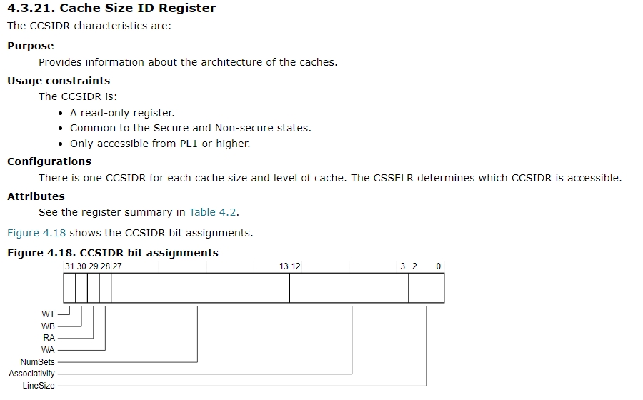
CCSIDR説明
| Field | Value | Function |
|---|---|---|
| WT | Indicates support for Write-Through | |
| 0 | Cache level does not support Write-Throug | |
| 1 | Cache level supports Write-Through | |
| WB | Indicates support for Write-Back | |
| 0 | Cache level does not support Write-Back | |
| 1 | Cache level supports Write-Back | |
| RA | Indicates support for Read-Allocation | |
| 0 | Cache level does not support Read-Allocation | |
| 1 | Cache level supports Read-Allocation | |
| WA | Indicates support for Write-Allocation | |
| 0 | Cache level does not support Write-Allocation | |
| 1 | Cache level supports Write-Allocation | |
| NumSets | Indicates the number of sets in cache – 1 | |
| Associativity | Indicates the associativity of cache – 1 | |
| LineSize | Indicates the cache line | |
| 0b001 | 8 words per line | |
| 0b010 | 16 words per line |
Level 1 Data Cache は、WB,RA,WA をサポートしています。
| Field | Value | Function |
|---|---|---|
| NumSets | 0x7F | 128 sets |
| Associativity | 0x03 | 4-ways |
| LineSize | 0x2 | 16 words per line |
Level 1 Data Cacheのサイズは、Line Size(16word) × sets(128) × ways(4) = 32KB となります。
Level 1 Instruction Cache は、RA をサポートしています。
| Field | Value | Function |
|---|---|---|
| NumSets | 0x1FF | 512 sets |
| Associativity | 0x01 | 2-ways |
| LineSize | 0x1 | 8 words per line |
Level 1 Instruction Cacheのサイズは、Line Size(8word) × sets(512) × ways(2) = 32KB となります。
Level 2 Unified Cache は、WB,RA,WA をサポートしています。
| Field | Value | Function |
|---|---|---|
| NumSets | 0x3FF | 1024 sets |
| Associativity | 0x07 | 8-ways |
| LineSize | 0x2 | 16 words per line |
Level 2 Unified Cacheのサイズは、Line Size(16word) × sets(1024) × ways(8) = 512KB となります。
キャッシュ構造の説明
Cortex-A7のキャッシュは、セットアソシアティブ(Set Associative)方式です。
キャッシュライン長をひとつのブロックとして、キャッシュをSet数×Way数のキャッシュブロックに分割します。そして、メモリとキャッシュ間はキャッシュライン単位に転送します。
例として、ライン長 16word 8 Set 2-Way アソシアティブキャッシュの構造を示します。
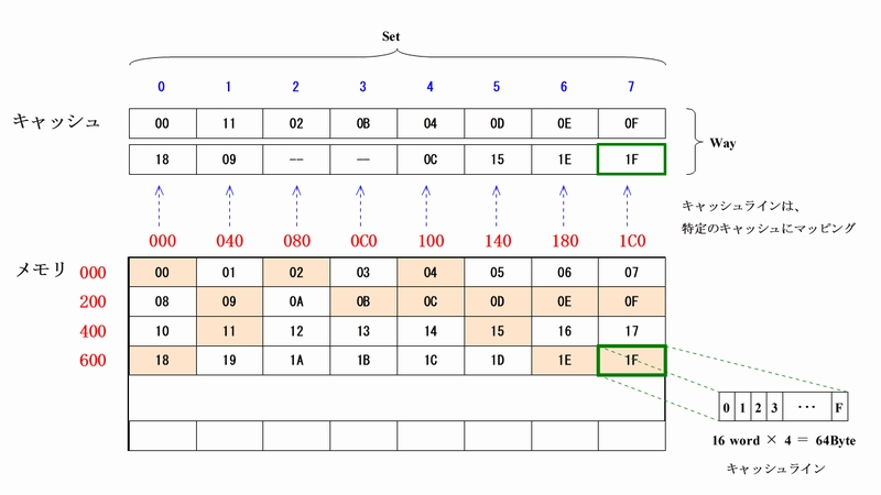
8 Set 2-Way アソシアティブキャッシュ
キャッシュラインは、16word×4=64 byte単位のブロックとなります。メモリのおのおのキャッシュラインは、特定のキャッシュにマッピングします。
- キャッシュ Set[0]は、アドレス0x000 ,0x200 ,0x400 ・・・ のキャッシュライン
- キャッシュ Set[1]は、アドレス0x040 ,0x240 ,0x440 ・・・ のキャッシュライン
- キャッシュ Set[2]は、アドレス0x080 ,0x280 ,0x480 ・・・ のキャッシュライン
- キャッシュ Set[3]は、アドレス0x0C0 ,0x2C0 ,0x4C0 ・・・ のキャッシュライン
- キャッシュ Set[4]は、アドレス0x100 ,0x300 ,0x500 ・・・ のキャッシュライン
- キャッシュ Set[5]は、アドレス0x140 ,0x340 ,0x540 ・・・ のキャッシュライン
- キャッシュ Set[6]は、アドレス0x180 ,0x380 ,0x580 ・・・ のキャッシュライン
- キャッシュ Set[7]は、アドレス0x1C0 ,0x3C0 ,0x5C0 ・・・ のキャッシュライン
アドレスの中位3ビット(0~7)がSetアドレス、アドレスの下位6ビット(0~63)がキャッシュライン内アドレスとなります。
アドレス0x0000(BLK-00)、0x0200(BLK-08)、0x0400(BLK-10)、0x0600(BLK-18)は、キャッシュ Set[0]にマッピングします。この例では、アドレス0x0000と0x0600にアクセスした例です。2-Wayキャッシュですので同一セットにマッピングしたキャッシュラインを2個までキャッシュに格納することができます。キャッシュ Set[0]は、BLK-00とBLK-18を格納しています。
次に、アドレス0x0200(BLK-08)をアクセスするとキャッシュの置換アルゴリズムによりキャッシュ Set[0]のひつとのキャッシュを解放して、キャッシュ Set[0]にBLK-08を格納します。
まとめ
Raspberry Pi2のRaspbian OSのキャッシュメモリ構造を調べました。
- Level 1 Data Cacheは、16wordライン長で4-Way 128セットアソシアティブ構造で32KB搭載しています。
- Level 2 Unified Cacheは、16wordライン長で8-Way 1024セットアソシアティブ構造で512KB搭載しています。
さて、最適化実装する場合はどんな点に留意すれば良いでしょうか?またの機会に考えてみます。
ピンバック: Raspberry Pi3 (BMC2837)のキャッシュ設定を調査 | ある計算機屋さんの手帳